Neural Probe
Design, Fabrication, & CharacterizationBiomedical Microsystems Laboratory, USC
- Supervisor
- Professor Ellis Meng
Publications
Barrera, N.D., Nguyen, T.D., Ramirez, E., Leach, C.R., Abbasi, N., Molisch, A., Sideris, C., & Meng, E. Implantable Flexible GHz Waveguide for High Data Throughput Neural Recording Interfaces. Neural Interfaces 2025 Conference, June 2025.
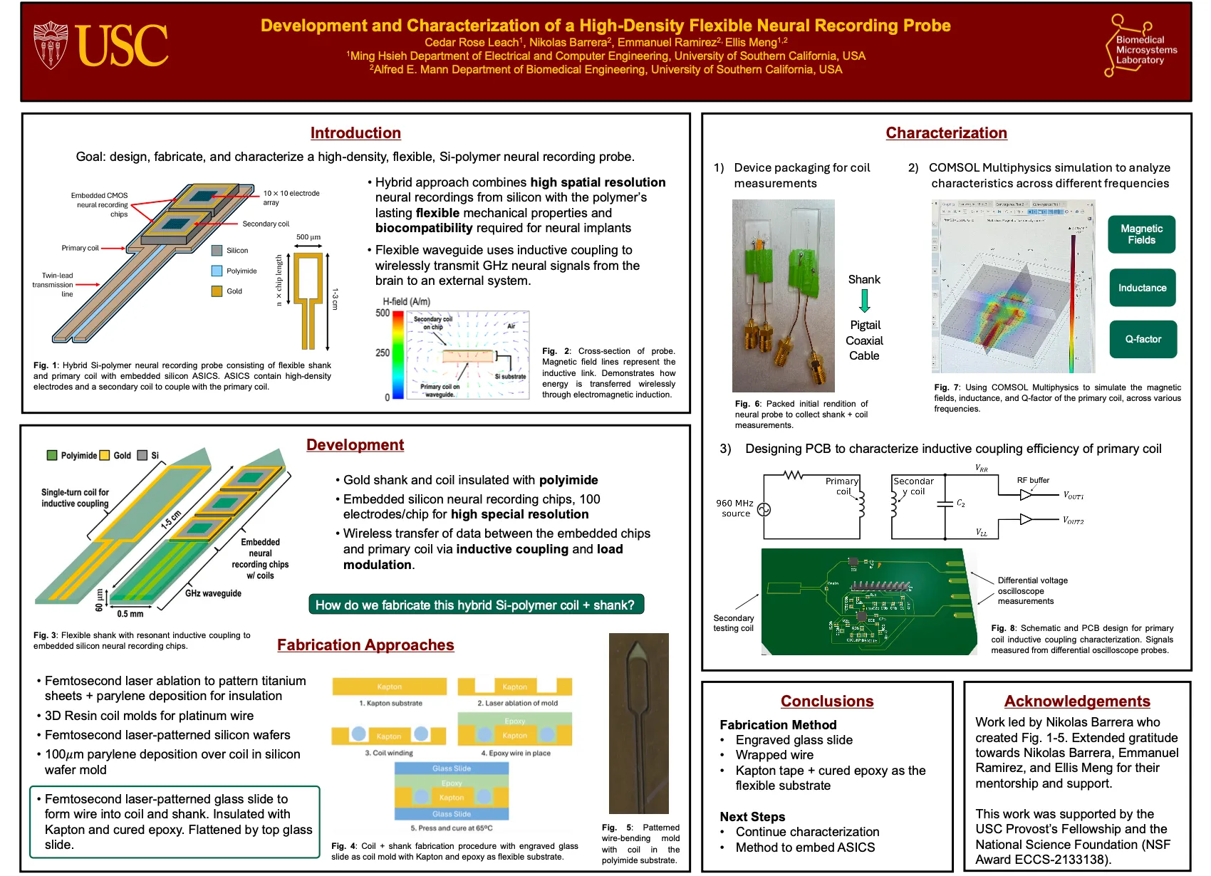
Leach, C.R., Barrera, N., Ramirez, E., & Meng, E. Development and Characterization of a High-Density Flexible Neural Recording Probe. Research symposium poster, University of Southern California, 2025.
Since July 2024, I’ve been helping to design, fabricate, and characterize a hybrid silicon-polymer neural recording probe.
This neural probe aims to combine the flexibility of polymer-based neural interfaces and the high electrode density of silicon-based neural interfaces. This hybrid approach enforces high spatial resolution neural recordings while maintaining flexible mechanical properties and biocompatibility required for neural implants. To create this novel neural probe, I am assisting in developing and testing the fabrication procedure for the flexible shank.
I joined this lab last summer after a month of training in semiconductor fabrication processes in the cleanroom. I was able to translate this knowledge of nanofabrication to the lab’s development of neural interfaces. I truly enjoy the process of creating this device. It’s a ton of trial and error, brainstorming different fabrication methods and figuring out what works and what doesn’t. I can think of at least six different fabrication approaches that we have undertaken, and each approach has many different variations - tweaking the mold CAD file, or the material of the coil, or the method of transferring the coil to the substrate, or the coil-forming strategies.
There are standard fabrication processes for creating neural probes (e.g. photolithography, deposition, etching, liftoff). However, our project requires a new fabrication approach since we are dealing with a much thicker layer of conductive material.
Throughout the process of brainstorming, designing, fabricating, and characterizing the neural probe, I have gained valuable knowledge and honed a variety of skills, including:
Femtosecond Laser Ablation
To precisely pattern coils from a titanium sheet for one rendition of the neural probe.
Fusion 360 CAD
Created the mold for forming a wire into the desired shape of the primary coil. Developed multiple mold variations to optimize both the coil’s geometry and the efficiency of the wire-forming process.
K-Layout
Designed 2D coil patterns for fabrication on silicon wafers.
Device Packaging
Soldering and coil molding to create the primary coil and neural probe shank. Attached SMA connectors for testing and measurements.
S-param Data Analytics
S to Z conversion to analyze impedance of primary coil and derivation of inductance.
COMSOL Simulations
Learned COMSOL, simulating magnetic field and inductance properties of the probe to optimize coil performance.
Parylene Deposition & Etching
Worked in the cleanroom depositing parylene for various renditions of the probe. Parylene serves as an insulator and a substrate for the probe.
Analog-to-Digital Converter (ADC)
Researched and selected ADC eval boards as to digitize probe data. Focused on specifications such as sampling rate & bit resolution.
PCB Design
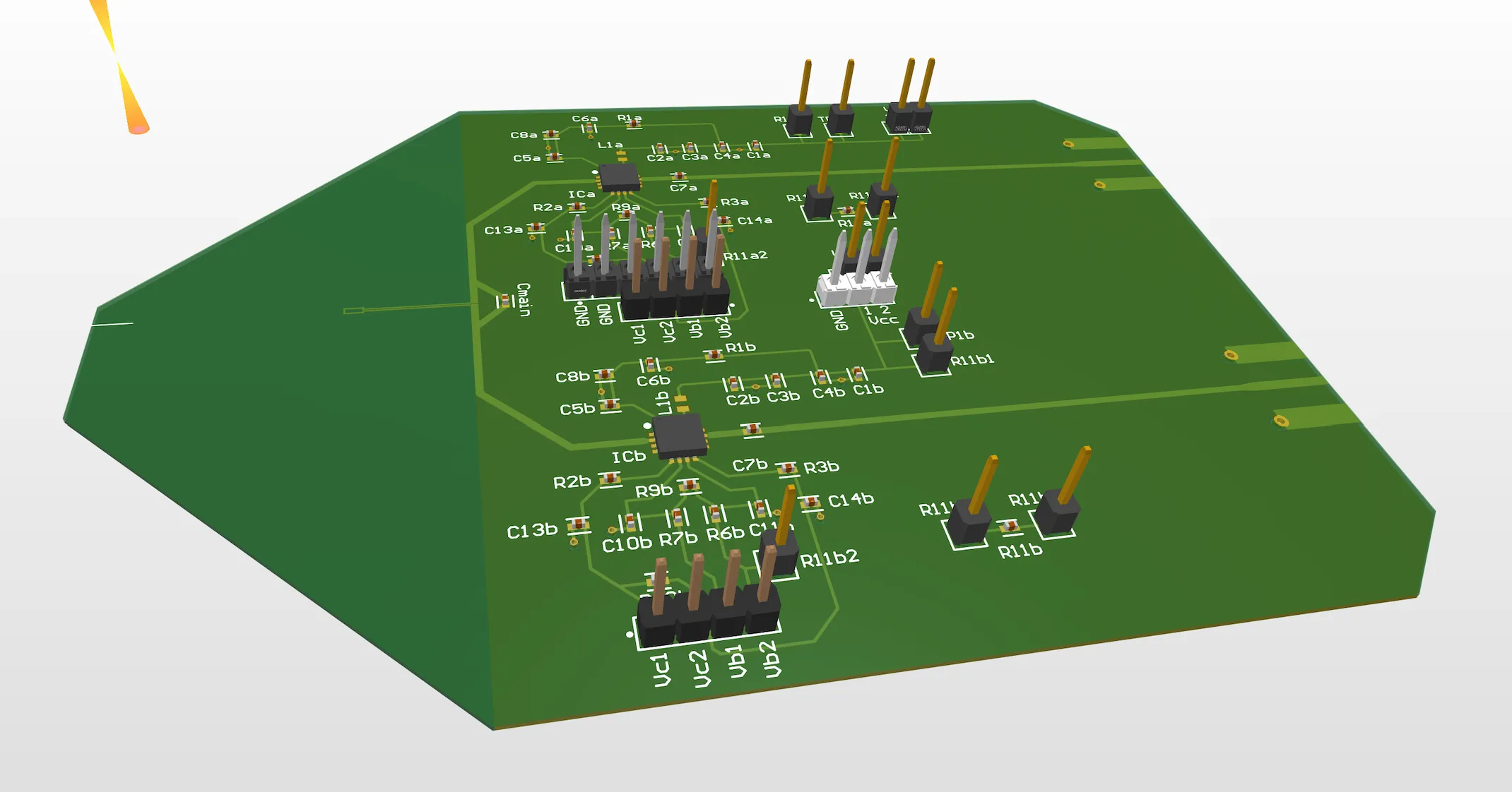
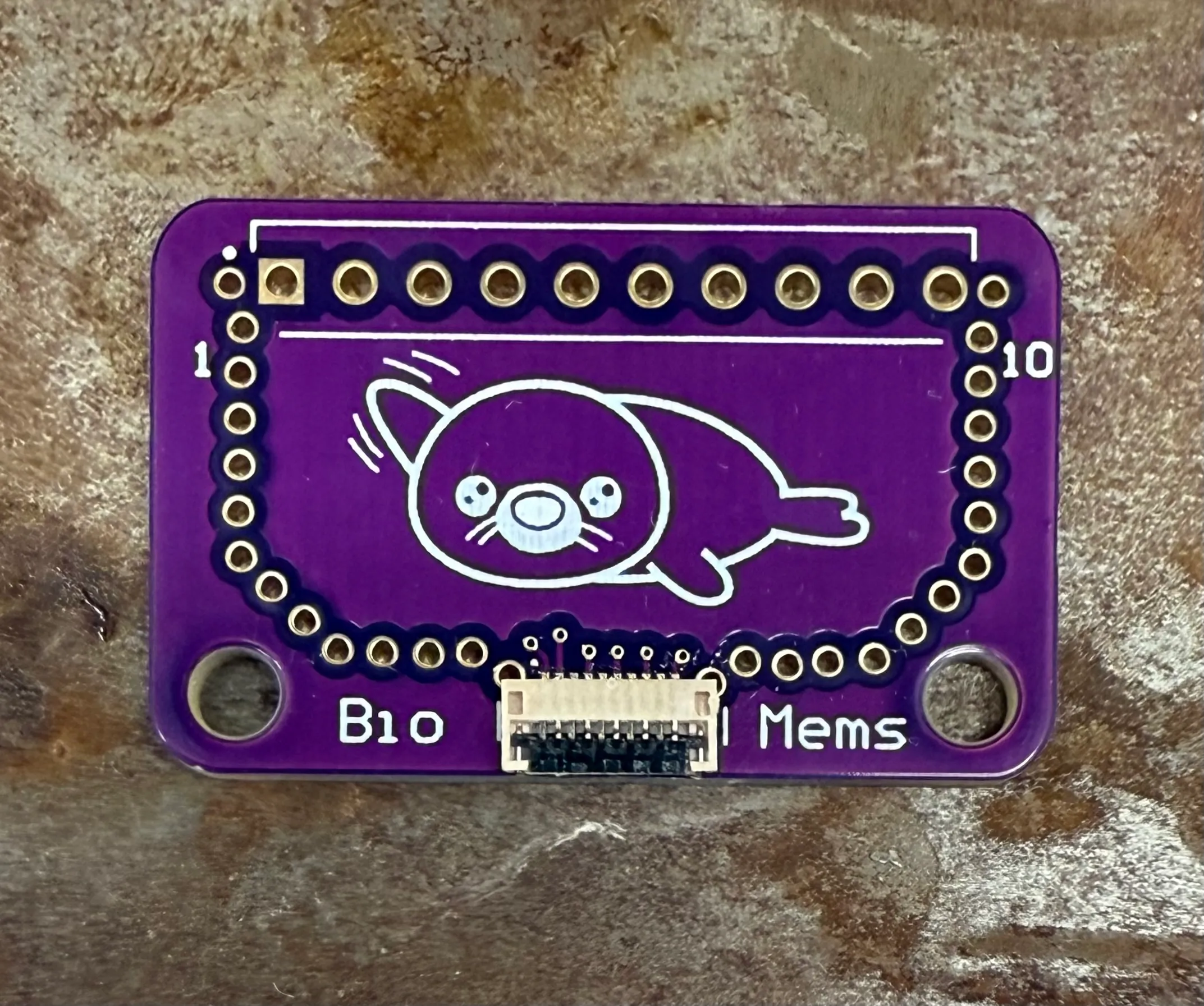
Designed two custom PCBs. The latest is a testing tool for evaluating inductive coupling efficiency of the neural probe’s primary coil. I configured dual RF amplifiers to measure voltage differentials across the ports and calculated trace widths for impedance matching. The second board just adapts a ZIF connector to Molex pins, but I made it 10x cooler with cute seal saying hi.
Photos and figures